Analyzing reflash routines Part 1 (Jaguar AJ27 specific)
In the last post, we created a Motorola BDM interface to extract code/data from both processors TPU EEPROM, SLIM area (overall processor configuration), and main EEPROMS.
Ghidra “.bin” versions of the 4k bytes of TPU code can be found in this repository. “F27xC_LNF1410AB_TPU” and “F27xD_LNF1410AB_TPU” are CPU1 and CPU2 TPU bootcode for a Y5 variant from an LNF1410AB firmware load. “F27xC_LNG1410BD_TPU” and “F27xD_LNG1410BD_TPU” are CPU1 and CPU2 TPU bootcode for a Y6 variant from an LNG1410BD firmware load.
By analyzing the configuration of the SLIM block, and reviewing the TPU EEPROM code, we can start building a picture of how the reflash process is achieved.
After a reset, the processor beings bootstrap operation by fetching the reset vectors, which provide values for key registers, as follows:

The processor then begins fetching instructions from the 20 bit address pointed to by PK:PC
The reset vector can be provided by one of the EEPROM blocks, if so configured. To do this, bit 12 (BOOT) of the module configuration register (MCR) is programmed to be low, which enables the 4 bootstrap words in the EEPROM module control block to be used as the reset vector.
Looking at the data extracted from the SLIM block for a couple of ECU modules, we see the following configurations for the EEPROM module configuration registers.
SLIM from an LNF1410AB ECU (Y5 variant - Five 32k flash EEPROM modules and one 4k TPU flash EEPROM)
| Address | Label | CPU1 value | bit 12 | CPU2 value | bit 12 |
|---|---|---|---|---|---|
| 0xff7c0 | FEE1MCR | 0x1ac0 | High | 0x1ac0 | High |
| 0xff7e0 | FEE2MCR | 0x1ac0 | High | 0x1ac0 | High |
| 0xff800 | FEE3MCR | 0x1ac0 | High | 0x1ac0 | High |
| 0xff820 | FEE4MCR | 0x1ac0 | High | 0x1ac0 | High |
| 0xff840 | FEE5MCR | 0x1ac0 | High | 0x1ac0 | High |
| 0xff860 | TFMCR | 0x0a00 | Low | 0x0a00 | Low |
SLIM from an LNG1410BD ECU (Y6 variant - Two 64k flash EEPROM modules, one 32k flash EEPROM module, and one 4k TPU flash EEPROM))
| Address | Label | CPU1 value | bit 12 | CPU2 value | bit 12 |
|---|---|---|---|---|---|
| 0xff780 | FEE1MCR | 0x1ac0 | High | 0x1ac0 | High |
| 0xff7c0 | FEE2MCR | 0x1ac0 | High | 0x1ac0 | High |
| 0xff800 | FEE3MCR | 0x1ac0 | High | 0x1ac0 | High |
| 0xff860 | TFMCR | 0x0a00 | Low | 0x0a00 | Low |
So in all cases, the TPU EEPROM flash block is configured to provide the reset vector.
Reviewing the values programmed for the TPU Bootstrap words 0-3 (at addresses 0xff870-ff876), in all cases above, these are:
- Word0 = 0x0bb3
- Word1 = 0x0000
- Word2 = 0x0ffe
- Word3 = 0x0000
Also reviewing the value programmed for the TPU EEPROM base address (at addresses 0xff864-ff866), in all cases this is 0x30000
This value of the reset vector causes the initial register values after reset to be: ZK:IZ = 0xb0000 SK:SP = 0xb0ffe PK:PC = 0x30000
So in all cases after a reset, program execution starts at address PK:PC = 0x30000, which is the start address of the TPU EEPROM flash block.
Reviewing CPU1 (IC501) TPU code, the rough outline of the program is as follows:
- Configure I/O ports, Queued ADC, SRAM, CAN controller
- (One notable aspect of the TPU firmware is that it does not use the SRAM as storage, rather it uses the Canbus controller message storage as a makeshift RAM area)
- Read Flash Comms Control Port (FCCP), and Flash Program Voltage (VFP)
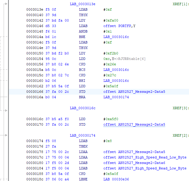
FCCP is mapped to PortF, bit 0, which is tested at line 30148.
VFP is read by ADC AN50, which is loaded at line 30154, and checked against lower value of 0x026e and upper value of 0x027c.
Since there is a resistive divide-by-4 before the ADC, these values translate to the following voltages:
(622/1024) * 20 = 12.15V, and (636/1024) * 20 = 12.42V
If FCCP is high, or VFP is not in the range 12.15- 12.42V then the value 0xa5f0 is stored in the RAM for message 2 data 5/6. Whereas if both FCCP is low and VFP is in range, then 0x5a0f is stored. Then at 30188 the stored value is retrieved and tested, with a conditional branch to 30e36.
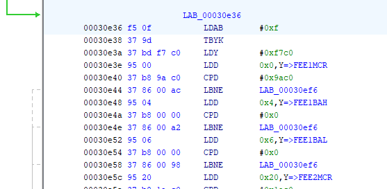
If there is a branch (FCCP high or VFP out of active range), firstly EEPROMs are configured, and then
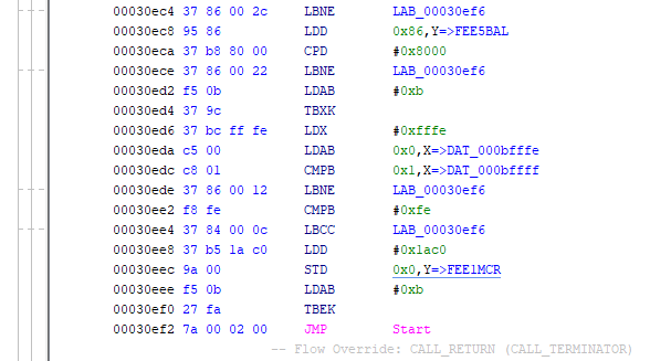
starting at 30ed2 the values stored at addresses 0xbfffe and 0xbffff are checked to be equal, and less than or equal to 254.
These are the erase and re-flash counters for the EEPROMs, so this checks that there have not been excessive reflashes (noting that the Motorola specification is maximum 100 reflashes, not 255).
EEPROM1 is then enabled (MCR = 0x1ac0) and then we have an unconditional “JMP Start” (address 0x00200).
In summary, this means that unless the FCCP pin is pulled low and flash programming voltage is applied to the VFP input, before the processor is reset, then the processor jumps to the standard ECU firmware program which starts at address 0x200.
If on the other hand, FCCP is low and VFP programming voltage is applied before the processor is reset, then execution continues within the TPU flash firmware. Note that FCCP will float high if there is no connection to it.
The conditioning circuit on the ECU regulates the flash voltage to 12.30V provided a high programming voltage is applied to VFP (~ 15.3V or more). Op-amp U405A uses the 5V reference on “+” input to switch Q407 on and off and regulate “FlashProg” voltage. Target voltage is 5 * 33.7/13.7 = 12.3V
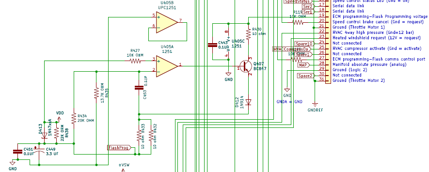
The circuit also includes aspects of the Motorola recommended conditioning circuit.
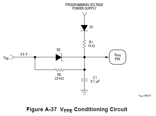
If execution of the TPU code continues, then some additional initialization takes place:
- Enable EEPROM1, configure Canbus controller, Serial port B, and RSPI (Ram buffered SPI between processors)
- RSPI is configured for single frame transfer
- Transfer from IC501 to IC601 (master to slave) 0xb13f0-0xb17f7 to 0xb17f8-0xb1bff
- Transfer from IC601 to IC501 (slave to master) 0xb13f0-0xb17f7 to 0xb17f8-0xb1bff
Then a loop is entered which executes the following high level functions
- (one time) After a short timeout, send 0 over serial port B to CPU2
- Check if a byte is received from CPU2 over the serial port B
- Check if a message is received over canbus (from ID 0x20)
- Check if software watchdog timer has counted down to zero, and if so reset some flags, and restart timer
- Use real time counter to maintain power supply hardware watchdog signal
The operations supported by this loop, and the corresponding operations executed in CPU2 TPU code, will be examined in the next post
