Extracting firmware code part 2
In order to operate the BDM interface via an Arduino, as introduced in the previous post, there are a number of processes that need to be coded. To recall, various Arduino input/output pins are used as follows:
- D7 is used to initiate a RESET signal to the target processor. By outputting logic high signal, the transistor is turned on and pulls the RESET signal low to initiate the reset process
- D6 is used to assert the BKPT signal low as part of forcing the target processor into BDM mode, so it initially is configured as an output. Since the same signal is also used as the SPI interface clock to transfer data, this output will also be used as an ‘auxiliary’ clock output to send/receive the first bit of the 17 bit BDM command. It is then disabled to allow the Arduino SPI logic to send the remaining 16 bits
- D5 is used to read the FREEZE signal, which is asserted high when BDM mode is activated by the target processor. So this needs to be configured as an input.
- D4 is used as an auxiliary MOSI (Master Out Slave In) signal, in order to send the initial bit of the BDM command. It is then disabled to allow the remaining bits to be sent using SPI
- D3 is used as an auxiliary MISO (Master In Slave Out) signal, in order to receive the initial bit of the BDM command.
So for initial configuration of the Arduino, we have the following
  //configure reset
  digitalWrite(7, LOW);
  pinMode(7, OUTPUT);

  //configure bkpt/dsclk
  pinMode(6, INPUT_PULLUP);

  //configure freeze
  pinMode(5, INPUT);

  //configure Aux MOSI
  pinMode(4, INPUT);

  //configure Aux MISO
  pinMode(3, INPUT);

  //configure arduino SPI interface
  // mode 3, CPOL=1, CPHA=1, DORD=0 for MSB first
  SPCR = 0x5d; //SPI no interrupt, mode 3, MSB first, 500 kbps clock (fosc/32)
  SPSR = 0x01; //SPI interface 500 kbps clock set SPI2X bit 0

  // SPDR is the SPI data register for byte input/output
  // SPSR bit 7 is the SPI flag which is set for completion of data read/write (collision flag is bit 6)

  digitalWrite(10, HIGH);
  pinMode(10, OUTPUT); //ensure slave select does not disable SPI operation
  pinMode(11, INPUT);  //MOSI for SPI disabled
  pinMode(13, INPUT); //SCK for SPI disabled
Next we want to initiate BDM mode on the processor. We do this by asserting the RESET signal, forcing BKPT to a low state, and then releasing the RESET signal.
  //initiate BDM

    digitalWrite(7,HIGH);  //assert reset
    pinMode(6, OUTPUT); //force bkpt low
    digitalWrite(6, LOW);
    DELAY_CYCLES(10);
    digitalWrite(7, LOW);  //release reset
Once we are in BDM mode, we want to be able to send BDM commands using the required 17 bit format. The basic packet format is shown below.

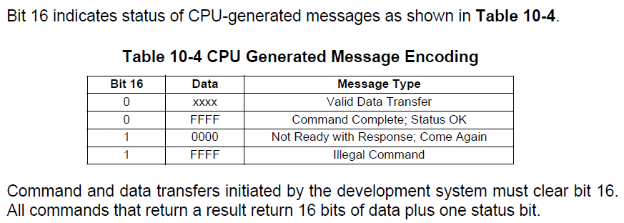
Definitions for the initial status/control bit (bit 16) are as below. Note for sending commands, bit 16 is always low.

To send a BDM command, the key processes are
- send the control bit and receive the status bit, by using the ‘auxiliary’ input/output pins
- send the 16 bits of data for the command, and receive and store the previous command response. The 16 bits are split into 2 bytes which are sent sequentially
- compute the status of the response message based on the status bit and the contents of the 16 bit response data
// sends a BDM command to MCU, and receives previous response
// command to send is passed in as 16 bit parameter
// response is stored in highRX and lowRX, and status is return value

int sendBDMCommand(unsigned int value)
{
    byte highVal = value >> 8;
    byte lowVal = value & 0xff;

    //prepare to send initial bit
    pinMode(11, INPUT);  //MOSI for SPI disabled
    pinMode(13, INPUT); //SCK for SPI disabled

    // force MOSI low and clock out initial bit
    digitalWrite(4, LOW);
    pinMode(4, OUTPUT);

    // create clock falling edge
    digitalWrite(6, HIGH);
    pinMode(6, OUTPUT);
    digitalWrite(6, LOW);
    //read status bit from MCU
    int statusBit = digitalRead(3);
    // clock rising edge
    digitalWrite(6, HIGH);

    //prepare for SPI
    pinMode(6, INPUT_PULLUP); //Aux clock floats high
    pinMode(4, INPUT); //Aux MOSI floats high (external pullup)
    pinMode(11, OUTPUT); //MOSI enabled
    pinMode(13, OUTPUT); //SCK enabled

    //send command
    highRX = sendSPIbyte(highVal);
    lowRX = sendSPIbyte(lowVal);

    //compute response message status
    if (statusBit == LOW)
    {
     if ((highRX == 0xff) && (lowRX == 0xff))
     {
       responseStatus = COMMAND_COMPLETE;
      }
     else
     {
       responseStatus = DATA_VALID;
     }
    }
    else
    {
     if ((highRX == 0x00) && (lowRX == 0x00))
     {
       responseStatus = NOT_READY;
     }
     else
     {
        responseStatus = ILLEGAL_COMMAND; // should really test if == 0000
      }
    }

  return responseStatus;
}
the above code relies on some constant definitions as below, to determine the status of the BDM command execution
const int DATA_VALID = 0;
const int COMMAND_COMPLETE = 1;
const int NOT_READY = 2;
const int ILLEGAL_COMMAND = 3;
and also a function to send/receive a data byte over SPI
//sends a byte over SPI, and waits until transmission complete before returning
byte sendSPIbyte(byte sendByte)
{
  SPDR = sendByte;
  while ((SPSR & 0x80) == 0) //wait for transmission to complete
  {
  }
  byte inByte = SPDR;
  return(inByte);
}
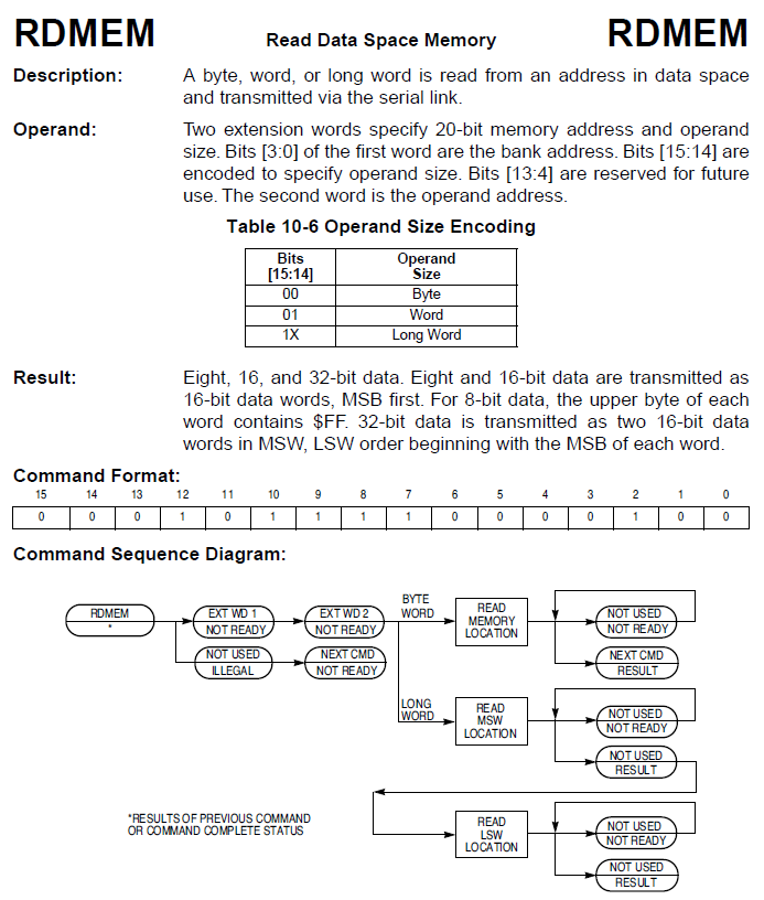
Armed with this generic routine to send a BDM data packet, we can now code functions to send the various BDM commands that are supported. For example, to read a byte/word/long word from data memory using the RDMEM command, the procedures are outlined below

Following the command sequence diagram above, to read a word from memory at address 0xnmmmm, the process is:
- Send the RDMEM command (0x01784)
- Send the first extension word, indicating a word is to be read, with bank address 0x000n (0x0400n)
- Analyze the response and check it is not “Illegal” (0x1ffff), if it is then flag an error by appropriate means
- Send the second extension word containing the operand address (0xmmmm)
- Send the next command, or NOP (No operation - 0x1789)
- Read the response, which will be the word value stored at the target data memory address
Sample code that executes the above is shown below. It also includes an extra feature which is notated as “pause while suspend operations flag is set”. This will be described later in the post.
//function to read a data memory word and return its value
unsigned int readDataWord(unsigned long targetAddress)
{
  boolean illegalResponse = false;
  int errorCount = 0;
  boolean notReady = false;

  unsigned int bankAddress = (targetAddress >> 16);
  unsigned int offsetAddress = targetAddress & 0xffff;
  unsigned int commandCode;

  // pause while suspend operations flag is set
  while (suspendBDMoperations)
  {
  };

  do
  {
      //Send RDMEM command
    unsigned int BDMResponse = sendBDMCommand(0x1784);

   //bank address
    commandCode = bankAddress + 0x4000;
    BDMResponse = sendBDMCommand(commandCode);
    illegalResponse = (BDMResponse == ILLEGAL_COMMAND);

    //if command received an illegal command response, then try again up to 3 times
    if (illegalResponse)
    {
      errorCount++;
    }
  }
  while (illegalResponse && (errorCount < 3));

  // if 3 failures, then show error condition and halt
  if (errorCount == 3)
  {
    showError();
  }

  //offset address
  commandCode = offsetAddress;
  BDMResponse = sendBDMCommand(commandCode);

  //receive the 2 bytes of data
  do
  {
    BDMResponse = sendBDMCommand(0x1789);
    notReady = (BDMResponse == NOT_READY);
  }
  while (notReady);

  unsigned int result = (highRX << 8) + lowRX;

  return result;
}
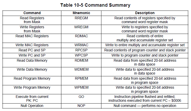
Functions for the other commands can be coded in a similar fashion. The list of available commands is shown below.

In order to download a significant amount of memory data such as the contents of 160kbytes of 68HC16Y5/6 flash data, the results need to be sent over the serial port to another device such as a PC. Since the Arduino has too little memory to store all the data at once, the simplest way of doing this is to read the data out one word at a time. This is a little slow, but gets the job done. Optimizations like downloading data in 1k chunks (or larger chunks if a different Ardiuno with more memory is used) can be added as required.
A function to do this is as follows
// function to read  block of data and send as bytes, preceded by start marker
void sendMemBlock(unsigned long startAddr, long numBytes)
{
  byte dataByte;
  unsigned long targetAddr = startAddr;

  for (long x=0;x<numBytes/2;x++)
  {
    unsigned int dataRead = readDataWord(targetAddr);
    byte byte1 = (dataRead & 0xff);
    byte byte2 = (dataRead >> 8);
    Serial.write(byte2);
    Serial.write(byte1);
    targetAddr = targetAddr + 2;
  }
}
In general putting together all these tools provides the functionality needed to extract the firmware. However, in the case of the Jaguar AJ27 ECU, with dual processors, there are a few nuances that need to be addressed. The first of these is that during the production run, the processor chip variant was migrated from a Y5 to a Y6. The Y5 uses 5 main EEPROM modules, each of 32kbyte. The Y6 uses 3 main EEPROM modules, 2 of size 64 kbytes and 1 of size 32 kbytes. In itself this is not a big difference, since they are mapped to the same address space in the AJ27 application (128k contiguous block and a separate 32 k block), so we read the same addresses independent of which chip version is present. The only key difference is that the control registers for the EEPROM blocks are mapped to different addresses, which makes sense since one chip has 5 control blocks and the other 3.
This brings us to the next point, which is that one of the EEPROM blocks is not enabled by default during reset and bootup of the chip. So if we are to read the data from all the EEPROM blocks, we need to re-enable the disabled one first. And since the control register addresses are different for the two variants, we need to know which variant we are dealing with. This can be determined by reading a test register in the overall control block for the processor (called the SLIM block). The value of the test register determines whether the processor is a Y5 or Y6, and allows us to know how to activate the disabled EEPROM block.
The final point is that the power supply for the ECU is subject to a hardware watchdog circuit, which must be continually reset by the main processor to avoid a power cycle reset. Similarly, the main processor monitors the secondary processor, and resets it if it fails to maintain its watchdog signal. Since initiating BDM mode freezes processor operation, this means that after a timeout period, a watchdog process will be triggered and reset whichever processor we are trying to extract data from, and BDM mode will be cancelled. As the watchdogs will trigger a reset in a few 10s of milliseconds, it does not leave much time to actually read out some data.
One possible solution to all of this is that the watchdog timeout can be predicted, since it occurs a roughly fixed time after BDM mode is triggered which freezes the processor operation. The Arduino can set a timer when BDM mode is initiated, and suspend memory readout just before the watchdog resets the processor. The Arduino can also detect this reset, and use this to trigger an interrupt that re-initiates the BDM mode. In this way, we simply suspend readouts while we re-initate the BDM mode, and then carry on.
Putting this all together, the first step is to add some setup code to determine whether the processor variant is Y5 or Y6, by reading the test register in the “SLIM” block
 //determine if the chip is a Y5 or a Y6
  unsigned int testVal = readDataByte(0xffa02);
  boolean isY6;

  if (testVal == 0xd0)
  {
    isY6 = true;
  }
We configure a ‘pin change’ interrupt on D6, which is the FREEZE signal. FREEZE is asserted high when BDM mode is triggered, and goes low when BDM mode is exited (when the processor is reset).
  //enable pin change interrupt on freeze pin
  PCMSK2 |= bit(PCINT21);
  PCIFR |= bit(PCIF2);
  PCICR |= bit(PCIE2);
Next we configure Timer1 in the Arduino, so that it will set a ‘suspend operations’ flag a fixed interval after BDM mode has been started.
//configure timer 1
 // Mode 4 CTC on OCRA
 // prescale 64 for 4 us tick
 // interrupt on OCA
 // timer set for 50 ms
  TCCR1A = 0;
  TCCR1B = 0xb;
  OCR1A = 12500;
  //start timer to anticipate next loss of BDM
  TCNT1 = 0;
  TIMSK1 = 2;
We configure an interrupt service routine for when the timer expires, which sets a ‘suspend’ flag, which can be used to pause the memory read requests in the main program.
 volatile boolean suspendBDMoperations;

//timer 1 output compare A interrupt
//set suspendBDMOperations flag
 ISR (TIMER1_COMPA_vect)
 {
   suspendBDMoperations = true;
 }
Finally, we create an interrupt service routine for the pin change interrupt, i.e. for when FREEZE goes high (start of BDM mode), and FREEZE goes low (loss of BDM mode). On entering BDM mode, we enable the disabled EEPROM block, reset the ‘suspend operations’ flag, and start the suspend timer. On losing BDM mode, we execute the process to re-enable BDM mode.
// pin change interrupt on pin D5 (freeze)
// detects loss of BDM, and re-initiates BDM
 ISR (PCINT2_vect)
 {
   boolean freeze;
   DELAY_CYCLES(5); //let settle
   freeze = (digitalRead(5) == HIGH);

   if (freeze)
   {
     // force MOSI low and clock out initial bit
    digitalWrite(4, LOW);
    pinMode(4, OUTPUT);
    DELAY_CYCLES(10); //let settle
    digitalWrite(6, HIGH); //rising clock pulse
    DELAY_CYCLES(10); //let settle
    pinMode(6, INPUT_PULLUP); //clock floats high
    pinMode(4, INPUT); //MOSI floats high (external pullup)

    // use SPI to clock out 16 bit message - send NOP
    pinMode(11, OUTPUT); //MOSI enabled
    pinMode(13, OUTPUT); //SCK enabled

    sendSPIbyte(0x17);
    sendSPIbyte(0x89);

    suspendBDMoperations = false;

    //start timer to anticipate next loss of BDM
    TCNT1 = 0;

    // add any operations required after reset here
    if (isY6)
    {
      writeDataWord(0xff780, 0x1ac0); //this flash block is not enabled after reset
    }
    else
    {
      writeDataWord(0xff7c0, 0x1ac0); //this flash block is not enabled after reset
    }
   }
   else
   {
    //re-initiate BDM
    pinMode(11, INPUT);  //MOSI for SPI disabled
    pinMode(13, INPUT); //SCK for SPI disabled
    pinMode(6, OUTPUT); //force bkpt low
    digitalWrite(6, LOW);
    digitalWrite(7,HIGH);  //assert reset
    DELAY_CYCLES(10);
    digitalWrite(7, LOW);  //release reset
  }
 }
A complete implementation of the Arduino code can be found here. The Arduino program reads out the entire 160 kbyte of flash memory, plus the 4k of TPU memory, plus the configuration of the ‘SLIM” block. A rudimentary PC program written in the Processing language is also posted in the repository, which receives the memory readout over the serial port, and saves the resulting file in the proprietary Jaguar “.b68” format. Note however that a special loader will be required for this file, since it is larger than a standard 160 kbyte file as it includes the TPU EEPROM and SLIM block data. Note also that since the Arduino and Processing IDEs are based on the same basic IDE, it is best not to have both open at the same time, to avoid conflicts on serial port allocation.
