Extracting firmware code part 1
Whilst analyzing an ECU is important, it is of limited value without the ability to modify code and data. Most ECUs can be re-programmed, but the procedure is usually implemented by a manufacturer tool, and may not be easy to use for purposes other than intended by the manufacturer.
In the case of the Jaguar AJ27 ECU being studied here, the question arises “How are the CPUs reflashed?”
Considering the architecture of the CPU, a few of the considerations are:
- Obviously it is not possible to run code contained in an EEPROM whilst simultaneously erasing and reprogramming it, especially since the EEPROMs on this processor can only be erased as a single block.
- Even though there are multiple EEPROMs in the processor, so that one could hold code while another is erased and reprogrammed, this would be inefficient. It would also require EEPROMS to be reprogrammed twice, which is undesirable because this generation of flash EEPROMS has a very limited number of erase/reprogram cycles, specified as a 100 cycles.
- If the reflash program is not contained in the main EEPROMs, where is it? It could either be loaded into RAM (7k size), or could be contained in the TPU EEPROM (4k size) as the only other possibilities.
- If it is in RAM, how is it loaded? If code was copied from main ECU EEPROM into RAM, and then program execution jumped to that code in RAM, it should be relatively easy to find. The are no traces of such code in the main EEPROM firmware
- The EEPROMs are 32k or 64k in size, whereas the RAM in the CPU is 7k in size. So any re-flash program is going to have to load the EEPROM reprogram data into RAM in smaller chunks
- The manufacturer tool database of EEPROM code files lists 4 files per ECU version. These are labeled MainBoot, MainCal, SubBoot, and SubCal. Since we already have discovered that MainCal and SubCal are the 160k files for the two ECU processors, it would seem that MainBoot and SubBoot are likely related to re-flash. Reviewing these files reveals that they are to be loaded starting at address 0xb0000 (which is the configured start address for RAM), and are about 5k and 4k in length (so fitting within the RAM memory space)
Reviewing the above points, it seems likely that re-flash boot code is contained in the TPU EEPROM, and this boot code is used to load the MainCal and SubCal programs into RAM. These programs will then execute the actual re-flash procedure. A quick analysis of MainBoot and SubBoot suggests that this is indeed the case, and that they receive commands and data over Canbus in order to execute these processes.
Regarding the TPU EEPROM, an initial question is whether there is any access of this memory space from the main ECU firmware. From initialization routines, we know the TPU EEPROM is mapped to memory space base address 0x30000. From IC501 (CPU1) there are 3 accesses.

At 4d8, if word value at 30ffa != 0xa5a5 then the code skips configuration of the Queued Analog to Digital Converter module. The ECU won’t function properly if the QADC is not configured, so clearly the TPU EEPROM must be programmed with at least a specific word (0xa5a5) at this location. At 27b0, if word value at 30ffc != 0xaa55 then the CPU skips a test of QADC operation. And at 1ef9c, if word value at 30ffa != 0xa5a5 then the CPU skips a checksum calculation for TPU EEPROM. Checks performed by IC601 (CPU2) are essentially similar.
The next question is how to obtain a copy of the code stored in the TPU EEPROM. There is one utility provided by the firmware to read memory data out on the Canbus, but the allowable addresses to be read exclude the TPU EEPROM. In the absence of other options, the only way forward is to use the debug port on the CPU, which for our target CPU (68HC16) is called the Background Debug Mode (BDM) interface. Other processor families may call the debug port a JTAG port, Serial Wire Debug, etc.
Implementation of the BDM interface, at least for the basic purpose of reading memory data (rather than the more advanced functions such as triggering breakpoints), is fairly simple, and requires two basic functions:
- Creating the appropriate signals to force the processor into BDM mode
- Implementing the interface to be able to query the processor and read/write memory locations
The BDM interface uses 10 connections, although for the basic purposes above, only 6 are needed (RESET, BKPT/DSCLK, FREEZE, DSI, DSO, GND). The recommended naming/numbering is shown below, and these connections are available as solder pads on the ECM PCB for both processors.
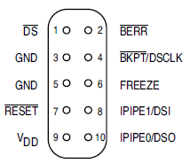
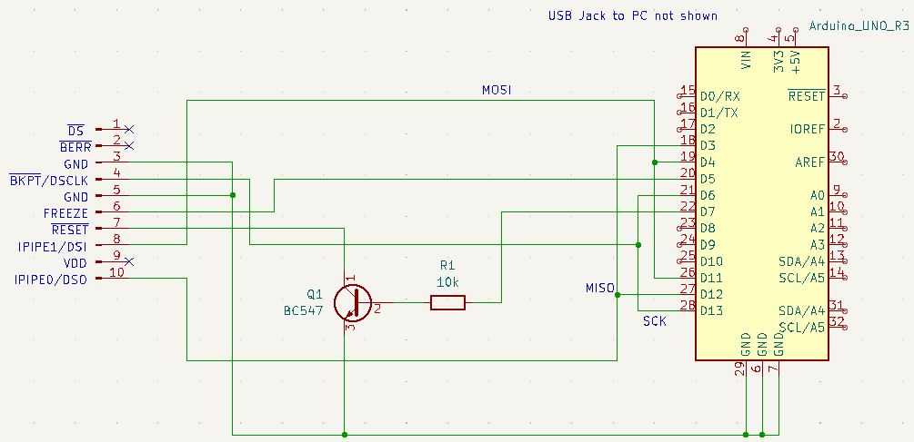
One way of implementing the above is to use an Arduino board (such as an Arduino Uno R3), combined with a basic circuit of one transistor and one resistor.
The procedure to force the processor into BDM mode is detailed below.
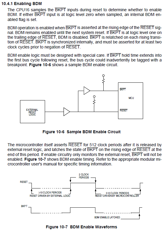
Referring to the above schematic, the NPN transistor pulls the reset signal low when output D7 is asserted high. The use of a transistor also allows the CPU to internally pull the Reset signal low, which is a requirement. The output D6 allows the BKPT signal to be asserted low, and D13 (SCK) will be disabled (tri-state) while this is done to avoid conflicts. D5 allows the FREEZE signal to be read, since this is asserted high to confirm that BDM mode has been activated.
The data interface to execute BDM commands is basically the same as a standard SPI interface (Serial Peripheral Interface) except that it uses a 17 bit data packet instead of the usual 8 or 16 bit packet. The ardunio SPI interface, configured for 16 bit operation, can still be used, but is supplemented with input/outputs D3, D4, and D6 which are used to send/receive the extra bit (‘bit banging’). The available BDM commands are summarized in the table below.
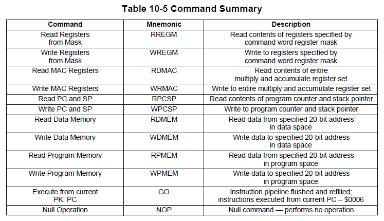
The key command that will be needed to extract the TPU EEPROM data is Read Data Memory (RDMEM). As a bonus, once this interface is coded, then other areas of the processor can be read and extracted. This will allow the reset configuration of the processor to be determined (such as the where to start code execution after a reset), as well as extraction of all other firmware, which will allow the particular firmware version on a sample ECU to be captured.
In the next post, I will go over some sample Arduino code that will provide the capabilities to read the memory contents from the processor.
