Annotating a firmware file in Ghidra
In this post, we will look into more detail of an AJ27 CPU firmware file. We will review how to add appropriate memory blocks and address labels to make the code easier to interpret. We will also examine how the CPU is configured for this particular AJ27 application.
Labeling registers
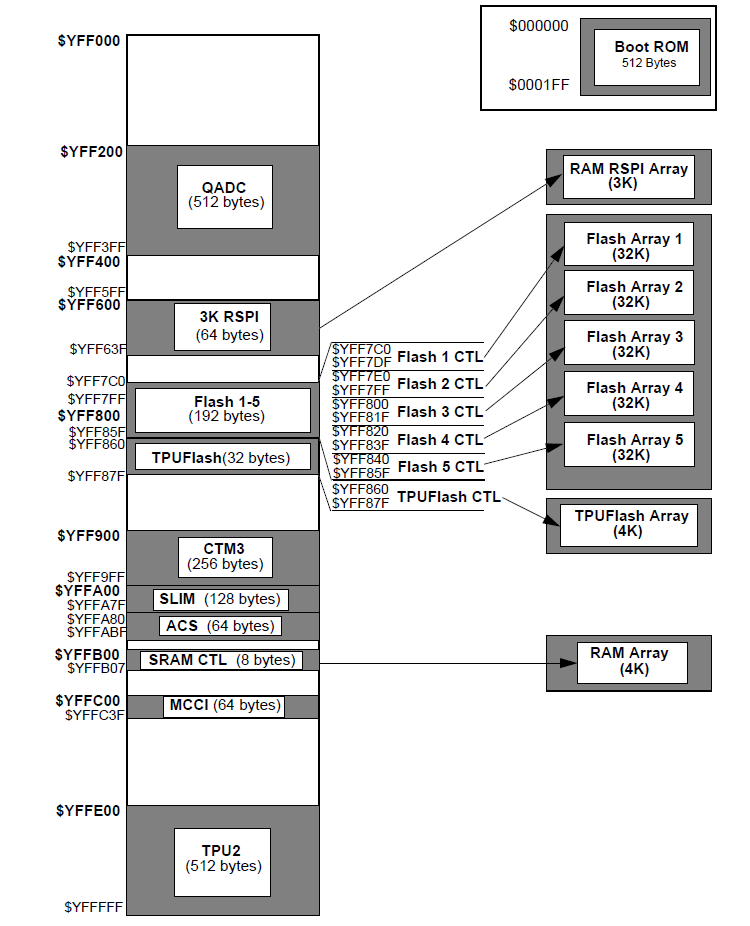
The Y5 and Y6 variants of the 68HC16 have a number of specialized modules in addition to the HC16 CPU core. The Y5 variant is illustrated below, which shows the modules and their mapping into the CPU address space. The Y6 variant is essentially the same as the Y5 except for the configuration of the main flash array.
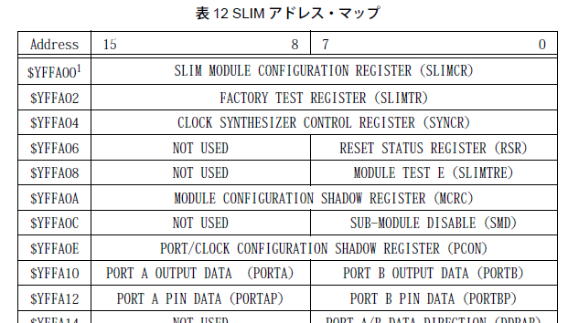
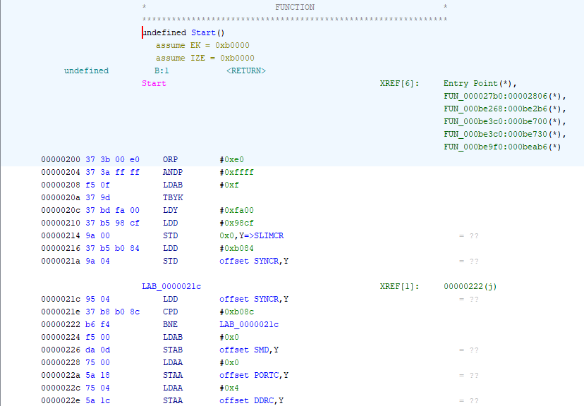
Each module has a number of registers that allow it to be configured, monitored, and controlled, and are either 1 byte or 1 word (2 bytes) in length. The memory locations of these registers are at fixed addresses, which means we can create a script in Ghidra, or a method in a loader module, to add labels to these addresses. This improves code readability, because Ghidra will replace the address shown in the code listing window with the applied labels. This is shown below for an example of the SLIM module being configured. A register address, such as 0xffa00 for the SLIM Configuration register, is replaced with the text “SLIMCR”.
The loader module reviewed in the previous post is written to automatically add these Y5/Y6 variant labels when importing a “.b68” AJ27 ECU flash file, because it knows that these files are specific to the ECU, and so the CPU must be a Y5 or Y6 (and not a Y3 or Z1 or R1, etc.), It does this with the method HC16Y5Labels().
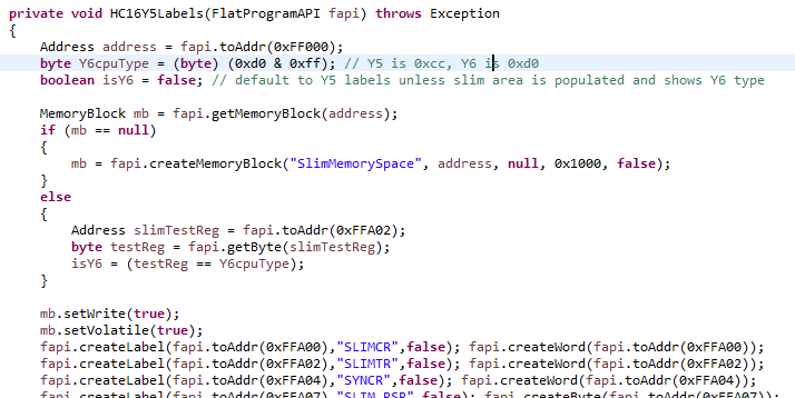
The labels are created using the Ghidra Flat API which provides methods to interact with code loaded into Ghidra. It is well covered in the “Basic Ghidra Scripting” chapter of The Ghidra Book. For example, for the SLIM CR register, we call two methods:
fapi.createLabel(fapi.toAddr(0xFFA00),"SLIMCR",false);
fapi.createWord(fapi.toAddr(0xFFA00));
The first creates the label “SLIMCR” for the address 0xffa0, and the second creates a word at this address, since the register is 16 bits, not 8 bits.
There are a few other tasks that this method undertakes:
- it creates a memory block at address 0xff000 of length 0x1000 bytes for all the modules, called “SlimMemorySpace”. This corresponds with the image at the start of this post which shows all modules are located between addresses 0xff000 and 0xfffff
- it determines whether the CPU is a Y5 or a Y6 variant, by reading the SLIM test register at address 0xffa02. (This is undocumented by Motorola, but from code analysis we can discover that the value stored here is 0xcc for Y5 variant and 0xd0 for Y6 variant. This information is used later in the method to determine which flash array labels to configure, since they differ for Y5 versus Y6
- it sets the type of memory for “SlimMemorySpace” to volatile, because some registers can change their values depending on operation of the CPU, and so they cannot be relied upon to be set to any particular value. Ghidra needs to know this when performing various analysis functions.
Labeling interrupt vectors and interrupt service routines
Another area of the code we can label are the exception vectors for the HC16 CPU, which are always located at addresses 0x0000 - 0x001ff.
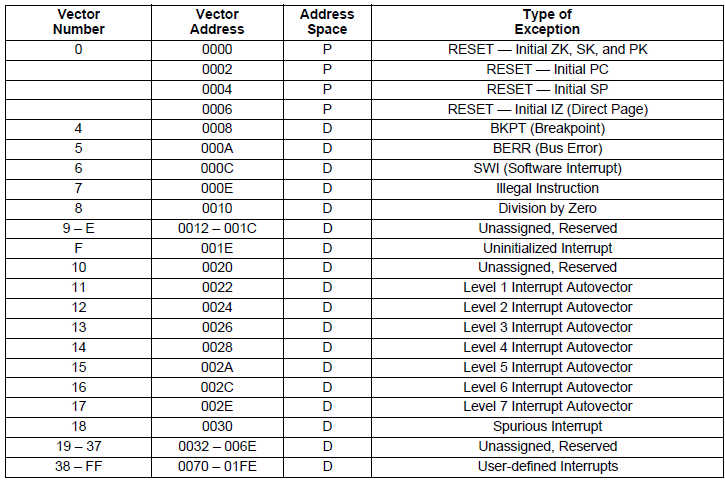
There are two tasks we can execute around these vectors. The first is to add a label to the vector location in memory.
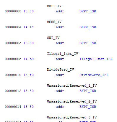
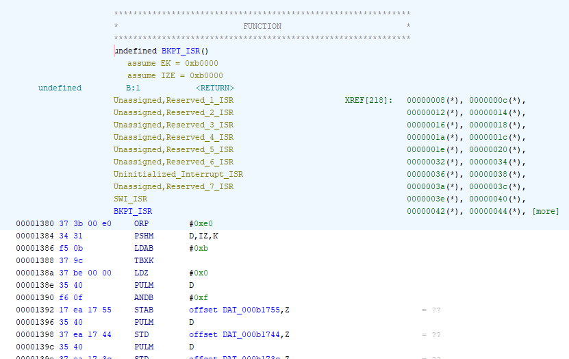
The second is, that provided that there is valid code loaded at the vector locations, we can read the values of the vectors, and create Functions at these locations, and label them with the name of the vector which pointed to them. For example, if the breakpoint interrupt vector, stored at address 0x00008 has the value 0x1380, then we can read this value, and create a Function at the address 0x01380, and give it the label BKPT_ISR to show this is the interrupt service routine for the BKPT interrupt.
We can create a table of the vector names and addresses
	private void HC16InterruptVectorsISRs(FlatProgramAPI fapi) throws Exception
	{
		// label interrupt vectors, and use vector to create function at interrupt service routine location
		String[][] vectorsData = {
				{"a", "BERR"},
				{"c", "SWI"},
				{"e", "Illegal_Inst"},
				{"10", "DivideZero"},
				{"12", "Unassigned,Reserved_1"},
				{"14", "Unassigned,Reserved_2"},
				{"16", "Unassigned,Reserved_3"},
				{"18", "Unassigned,Reserved_4"},
				{"1a", "Unassigned,Reserved_5"},
				{"1c", "Unassigned,Reserved_6"},
				{"1e", "Uninitialized_Interrupt"},
				{"20", "Unassigned,Reserved_7"},
				{"22", "Level_1_Interrupt_Autovector"},
				{"24", "Level_2_Interrupt_Autovector"},
				{"26", "Level_3_Interrupt_Autovector"},
				{"28", "Level_4_Interrupt_Autovector"},
				{"2a", "Level_5_Interrupt_Autovector"},
				{"2c", "Level_6_Interrupt_Autovector"},
				{"2e", "Level_7_Interrupt_Autovector"},
				{"30", "Spurious_Interrupt"},
				{"8", "BKPT"}
		};

		for (String[] s : vectorsData)
		{
			createVector(fapi, s[0], s[1]);
		}
and then iterate through the table, adding labels to the vectors, and creating an interrupt service routine function at the location pointed to be the value of each vector
	void createVector(FlatProgramAPI fapi, String addr, String name) throws Exception
	{
		Address address = fapi.toAddr(addr);
		Data pointer16 = fapi.getDataAt(address);
		if (pointer16 == null)
		{
			pointer16 = fapi.createData(address, Pointer16DataType.dataType);
		}

		Symbol sym = fapi.getSymbolAt(address);
		if (sym != null)
		{
			fapi.removeSymbol(address, sym.getName());
		}
		fapi.createLabel(address,name+"_IV",false);

		Address funAddress = (Address) pointer16.getValue();
		Function fun = fapi.getFunctionAt(funAddress);
		if (fun != null)
		{
			fapi.removeFunction(fun);
		}
		fapi.createFunction(funAddress,name+"_ISR");
	}
The loader module reviewed in the previous post also automatically marks up an imported “.b68” file with the vector names and associated ISR functions.
Creating and labeling memory blocks
Moving on to labeling other modules, a challenge we have is that for several of them their location in memory is configurable, and is set at run time by the code. The base memory addresses for the RAM and EEPROMs, as well as the Canbus controller, fall into this category. (Note that for the EEPROMS, their base addresses can be inferred from the information in the “b68” file, so the loader uses that information to create memory blocks for the code) This means we have to review the AJ27 ECU code before we can create routines to apply the appropriate labels. Luckily, it seems that the configuration is consistent across all AJ27 code variants (various model years and regions of Jaguar XJ8, XJR, XK8 and XKR). Using the files for XKR US model years 2001-3, with naming format F27S?074.b68, we can see the from ghidra code listing the configuration of the various modules in the initialization code as follows:
        0000039e 37 b5 00 fb     LDD        #0xfb
        000003a2 9a 04           STD        offset SRAMBAH,Y
        000003a4 37 b5 00 00     LDD        #0x0
        000003a8 9a 06           STD        offset SRAMBAL,Y
4k RAM block (length 0x1000) base address high is 0xfb and low is 0x0000. So the 4k RAM block is mapped to address 0xb0000 (considering only the 20 bit address)
        000006ee 37 b5 fb 10     LDD        #0xfb10
        000006f2 9a 06           STD        offset RSRBAR,Y
3k RSPI RAM block (length 0x0c00) base address is 0xb1000. So all RAM is in a contiguous block from 0xb0000 to 0xb1bff
        00000378 37 b5 00 03     LDD        #0x3
        0000037c 9a a4           STD        0xa4,Y=>TFBAH
        0000037e 37 b5 00 00     LDD        #0x0
        00000382 9a a6           STD        0xa6,Y=>TFBAL
The 4k TPU flash EEPROM (length 0x1000) is located at addresses 0x30000 - 0x30fff
        0000027a 37 b5 f8 00     LDD        #0xf800
        0000027e 9a 60           STD        offset CSBARA,Y
The chip select A (for AN82527 canbus controller) is located at address 0x8000 with size 0x800, so addresses 0x80000- 0x807ff. In reality the AN82527 only has 256 addresses, so usable address space is 0x80000 - 0x800ff.
The final module of interest is the RAM-buffered SPI module.
        0000071c 37 b5 00 20     LDD        #0x20
        00000720 9a 1c           STD        offset RSIX0,Y
        00000722 37 b5 02 5e     LDD        #0x25e
        00000726 9a 1e           STD        offset RSIX1,Y
        00000728 37 b5 02 60     LDD        #0x260
        0000072c 9a 22           STD        offset RSIX3,Y
        0000072e 37 b5 04 9e     LDD        #0x49e
        00000732 9a 24           STD        offset RSIX4,Y

        0000087a 37 b5 00 20     LDD        #0x20
        0000087e 9a 04           STD        offset DAT_000b1004,Y
        00000880 37 b5 02 5e     LDD        #0x25e
        00000884 9a 06           STD        offset DAT_000b1006,Y
        00000886 37 b5 02 60     LDD        #0x260
        0000088a 9a 08           STD        offset DAT_000b1008,Y
        0000088c 37 b5 04 9e     LDD        #0x49e
        00000890 9a 0a           STD        offset DAT_000b100a,Y
The disassembly from 0x71c-732 above is the configuration for the master RSPI. The master CPU (IC501) sends to the slave CPU (IC601) from start address offset 0x20 to end address offset 0x25e. The master CPU (IC501) receives from the slave CPU (IC601) from start address offset 0x260 to end address offset 0x49e. Where these offsets are relative to the base address of the RSPI RAM block, which as above is configured to be 0xb1000.
The disassembly from 0x87a-890 above is the configuration sent from the master RSPI to the slave. The slave sends to the master from start address 0x20 to end address offset 0x25e. The slave receives from the master from start address offset 0x260 to end address offset 0x49e.
The upshot of all this is that the contents of the master IC501 RAM addresses 0xb1020 - 0xb125e are transferred into the slave IC601 RAM addresses 0xb1260-0xb149e. And the contents of the slave IC601 RAM addresses 0xb1020 - 0xb125e are transferred into the master IC501 RAM addresses 0xb1260-0xb149e.
The loader module reviewed in the previous post included an option to add file specific labels when importing a “.b68” AJ27 ECU flash file. If this is selected then the following tasks are executed:
- Determine what the file type is, based on the file name
- only if the file is a “Maincal”
- create memory block for AN82527 Canbus controller and add labels to this memory block
- If the file is a “Maincal” (for main CPU IC501) or “Subcal” (for sub CPU IC601)
- create memory blocks for TPU EEPROM, Main RAM, RSPI RAM
- Create interrupt vectors and ISRs for the various modules (like SPI, TPU2, etc.)
- label RSPI locations 0xb1020 and b0x1260 with notes on how blocks are transferred to the other CPU
			boolean addFileSpecificLabels = ((Boolean) options.get(0).getValue()).booleanValue();

			if (((fileType == AJ27fileType.MAINCAL) || (fileType == AJ27fileType.MAINBOOT)) && addFileSpecificLabels )
			{
				//file is a IC501 file
				mainCalLabels(flatAPI);
				AN82527Labels(flatAPI);
				if (fileType == AJ27fileType.MAINCAL)
				{
					calLabels(flatAPI);
					Address commentAddress = flatAPI.toAddr(0xb1020);
					flatAPI.setPlateComment(commentAddress, "RAM section from 0xb1020 to 0xb125f used to send\n data to sister processor IC601 via RAM buffered SPI");
					commentAddress = flatAPI.toAddr(0xb1260);
					flatAPI.setPlateComment(commentAddress, "RAM section from 0xb1260 to 0xb149f used to receive\n data from sister processor IC601 via RAM buffered SPI");
				}
			}
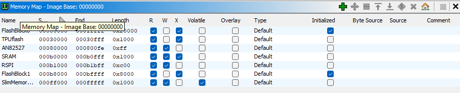
The results of the loader can be seen in ghidra using the “Display Memory Map” utility.
In the next post we’ll look at code disassembly, and how to identify data/tables versus code in a target file.