AJ27 Firmware Files
There are a few ways of obtaining a copy of the firmware from an ECU. One is to extract it directly from the ECU hardware, and there several techniques to do this, such as:
- Use a manufacturer diagnostic tool utility to download the data from the ECU, typically over OBD2 port, or proprietary port
- Access the memory chip directly, if there is one, such as on older ECUs that use a PROM/EPROM
- Access the debug/programming port of the CPU (JTAG, etc.) if the code is stored in the CPU in on-board/embedded flash memory. This may involve soldering or otherwise connecting directly to the ECU PCB
- For the AJ27 ECU, there are Motorola “BDM” debug/programming break out pads on the PCB for both CPUs
For Jaguar, the manufacturer diagnostic software tools are called SDD/IDS. These can be obtained from sources on eBay, etc. Browsing a software installation of SDD reveals a folder called “Flash”, such as in Jaguar > IDS > Flash. Within this folder there are some database files (.mdb extension). Study of these database files, (especially one called CAL_FILES.mdb) reveals the identity of the flash files for various car models/years
- e.g. for XKR Model year 2001+, there are 4 files, categorized as:
| Mainboot | Main Cal | Sub Boot | Sub Cal |
|---|---|---|---|
| F27SA074.b68 | F27SC074.b68 | F27SB074.b68 | F27SD074.b68 |
Copies of these files can be found in the “Flash” directory
We can examine one of these files, such as the “Main Cal / F27SC074.b68” file, using Ghidra. Create a new Ghidra project, and import the target file.
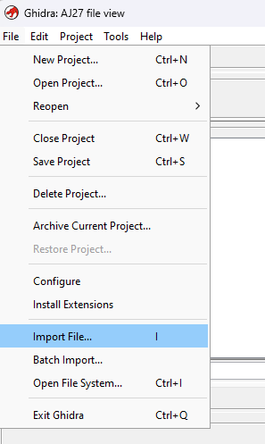
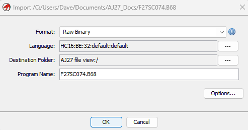
Select the target file, and click “Select File to Import”. The “Format” will default to “Raw Binary”, Select the “Language” to be the HC16 processor (assuming you have already installed the HC16 processor into Ghidra), and click “OK”
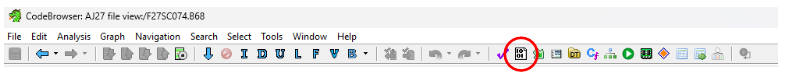
Ghidra will display an Import Results Summary screen. Double click on the file to open a CodeBrowser window, and click “No” when asked “Analyze”. Click on the “Display Bytes” icon to open the Byte Viewer window.
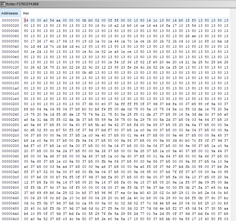
At the top of the Byte Viewer window, click on the spanner icon and change bytes per line from 16 to 32, and tick hex views.
What do we know about our target processor (HC16)?
- Exception vectors are stored in the first 512 bytes of memory:
- vector 0 sets initial extension registers values
- vector 1 is the initial program counter value
- Many instructions have the prefixes 0x17, 0x27, and 0x37
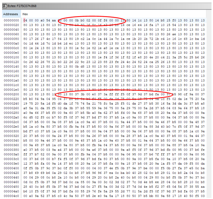
Here we can see that there are a number of bytes with value 0x37 starting at about address 0x209. And there is the value across two bytes of 0x200 at address 0x0a. In order to investigate further, we can try and disassemble code at the address 209, in case this is an instruction with a 0x37 prefix. Close the byte viewer, and select Navigation > GoTo…, and enter 209 to move to address 209 in the listing view. Right click on the Byte (37h) at address 0x209 and select Disassemble) (or press “D” on the keyboard).
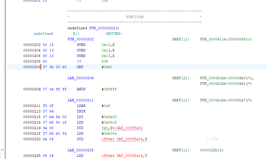
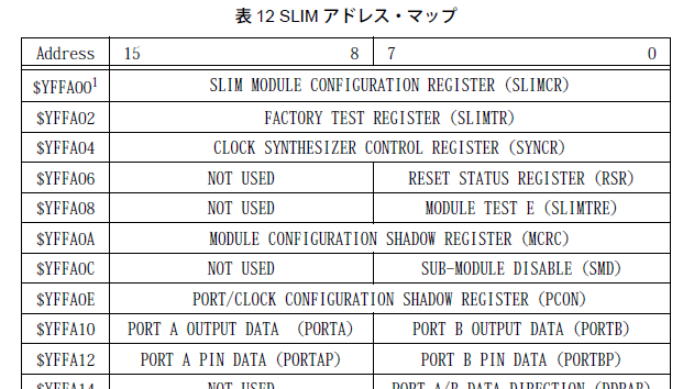
The disassembly looks reasonable. The Y index register is loaded with 0xffa00 (extension 0xf and main register 0xfa00) and the value 0x98cf is stored at address 0xffa00. Checking the HC16 Y5 variant manual, we see that we are writing to the SLIM module configuration register, which controls the overall configuration for the CPU, so this appears to be an initial configuration routine for the CPU. And the next instructions write to the same module, configuring the clock synthesizer control register, so it does indeed look like valid code starts here. Looking at code earlier than address 0x209 it does not disassemble cleanly, so it appears the code starts at address 0x209.
Scrolling down, at address 0x409 the code becomes messy.
The bytes at address 0x409 are 00 00 00 04 00. And the next byte is 0x37, which could be an instruction with a page3 prefix of 0x37. Something else that may not be a coincidence is that 0x409 is exactly 0x200 bytes after our start location. Going back to the hex viewer, and looking further ahead, we see something similar at address 0x80e.
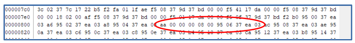
Here we see a pattern of bytes 00 00 00 08 00. And at address 0xc13 there is another pattern with 00 00 00 0c 00.

So we have code starting at 0x209. We know that for the HC16 processor, vectors occupy the first 0x200 bytes. So this suggests the vectors start at address 0x009. Looking here, we see that the first two vectors (at 0x009 and 0x00b) have the values 0x0bb0 and 0x0200. This would set the program counter to 0x0200. It is also possible that the first 9 bytes, before the start of vectors, are a file header. Also, the 5 byte sequences at 0x409, 0x80e, and 0xc13 (and so on) are block header for blocks of 0x400 bytes (= 1k bytes). Putting this altogether, and adding a bit more info from subsequent insights we have the following information on the “.b68” file format.
- 9 Byte initial header
- 04 00: block size (1k bytes)
- a0 00: number of blocks in file (160 blocks = 160 k)
- 54 aa: 16 bit checksum over file
- 00 00 00: load address for first block
- Initial 0x400/1k bytes
- 5 byte subsequent header/delimiters
- 00 00: delimiter
- 00 04 00: load address for next block
- Next 0x400 bytes
- and repeat for the “number of blocks” in the header
- Last two bytes in file are 00 00 delimiter
Armed with this information, we can write a Ghidra loader module to load flash files of “.b68” format into Ghidra for analysis, and this will be the subject of the next post.