AJ27 Firmware Introduction
In order to analyze the firmware stored in the ECU, there are few things that have to be done
- Obtain a copy of the firmware code
- Use a tool to analyze the code
- Understand the processor architecture and ECU connectivity to interpret what the code does
I’ll address these in reverse order, since there is no point in obtaining the code if there is no way of understanding what it does.
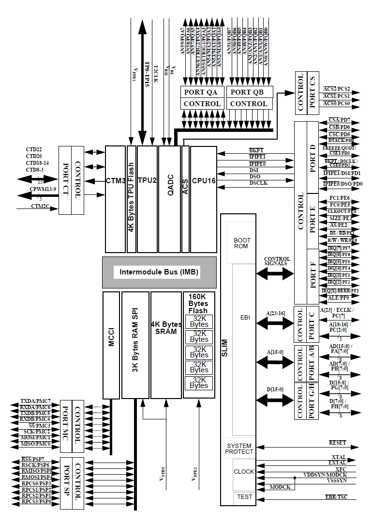
For the AJ27 ECU, we have established that the processors used are Motorola MC68HC916Y5/Y6, and in the previous post we looked at the connectivity of the CPUs to the various engine sensors and actuators.

The 68HC16 CPU is a 16 bit processor, clocked in this case at 24 MHz. Some highlights are:
- Addressing space is effectively 16+4 bits, i.e. 16 bit main address, and 4 bit extension address/page address.
- Flash memory is 164 kbyte, and is organized as either
- For Y5 variant, 5 blocks of 32k, 1 TPU2 block of 4k, each block with assignable base address in memory space
- For Y6 variant, 2 blocks of 64k, 1 block of 32k, 1 TPU2 block of 4k, each block with assignable base address in memory space
- RAM memory is 7k byte, organized as
- 4k general RAM with assignable base address in memory space
- 3k RAM for general use, or for RAM-buffered SPI, with assignable base address in memory space
- TPU2 module (Time Processor Unit2) - used for injector control, etc.
- CTM3 module (Configurable Timer Module 3) - used for ignition control, engine timing, etc.
- MCCI module (MultiChannel Communication Interface) - SPI and Serial interfaces, used for OBD2, inter-CPU bootstrap, O2 upstream sensors, knock sensors, etc.
- RSPI module (RAM-buffered SPI) - used for inter-CPU communications
- QADC module (Queued Analogue to Digital Converters) - used to read analog engine sensors
- Miscellaneous functions like system protection, general input/output, auxilary chip select (memory mapped external devices), etc.
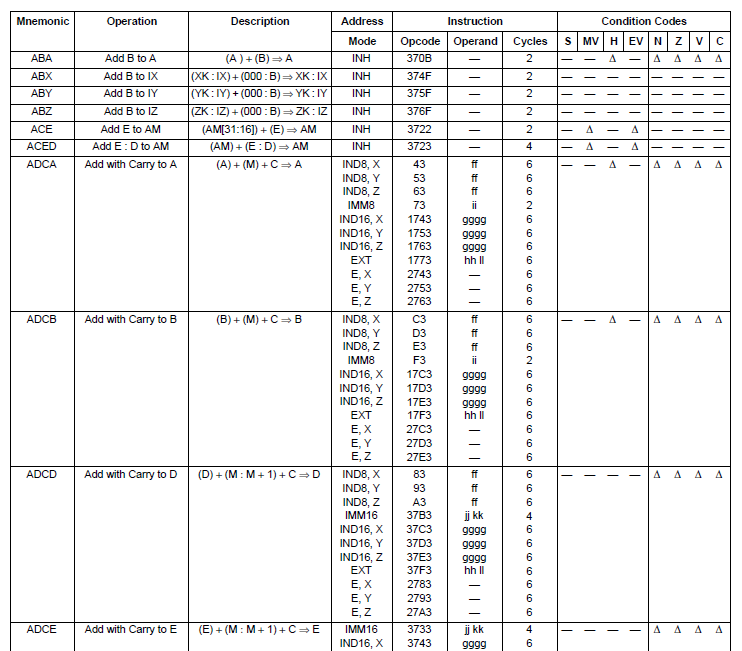
The 68HC16 instruction set is documented in the 68HC16 family reference manual which can be found here.

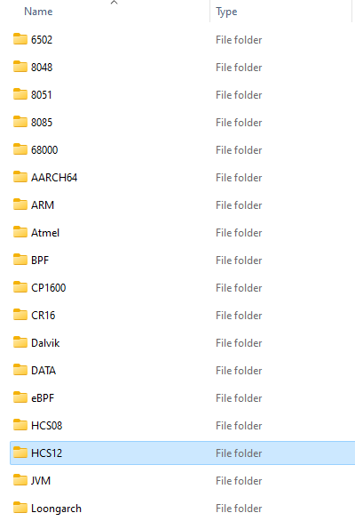
To analyze the code, there are multiple tools available. Two of the most popular are IDA - developed by hex-rays, or the free and open source tool Ghidra - developed by the US NSA. Ghidra, being free as well as highly capable, is an attractive option. Taking a look at the processors supported by Ghidra in version 11.1 (July 2024), by looking the “Ghidra > Processors” folder

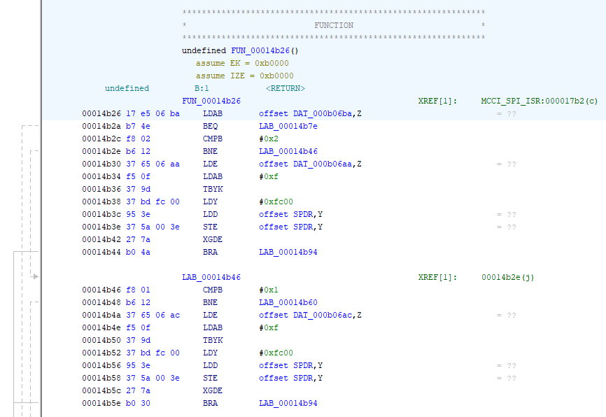
we find Motorola HCS08 (includes HC05, 08, S08) and HCS12 (includes 12 and S12) are supported, but no folder for the HC16. At first sight this rules out using Ghidra. However, Ghidra is open source, and has included great information on how to extend its functionality to add additional processor support. So before we can use Ghidra to disassemble the CPU code, and analyze the various functions, we need to write a processor module for the HC16 CPU. This requires writing a processor “SLEIGH” specification, which will be the subject of the next post. Once this is done, analysis can continue, providing views such as the snapshot below.

