AJ27 ECU Hardware Overview
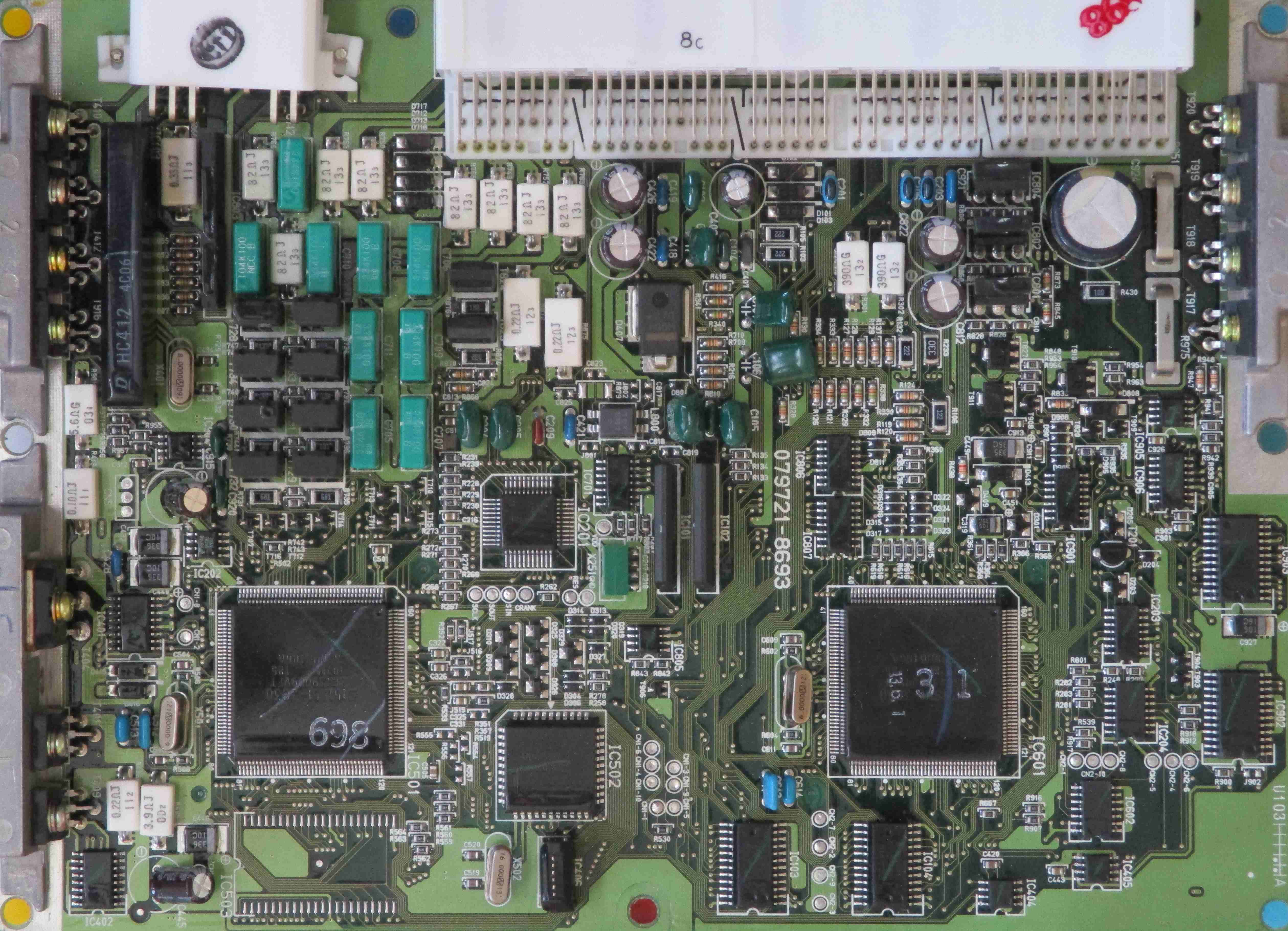
The AJ27 ECU is a typical design with a single PCB, heat sinks for power transistors at the sides, and all external connections at the top. The ECU was created and supplied by Denso as an OEM supplier to Jaguar. It was fitted to US model years 2000-03 of the Jaguar X100 and X308 models, and so was probably designed around 1997/98. It is an evolution of an earlier AJ26 ECU which was probably designed around 1995. Knowing this can sometimes help with component identification by focusing in on the components that were commonly available used in this era. The top side of the PCB has a number of surface mount integrated circuits, as well as a mix of surface mount and through hole components.
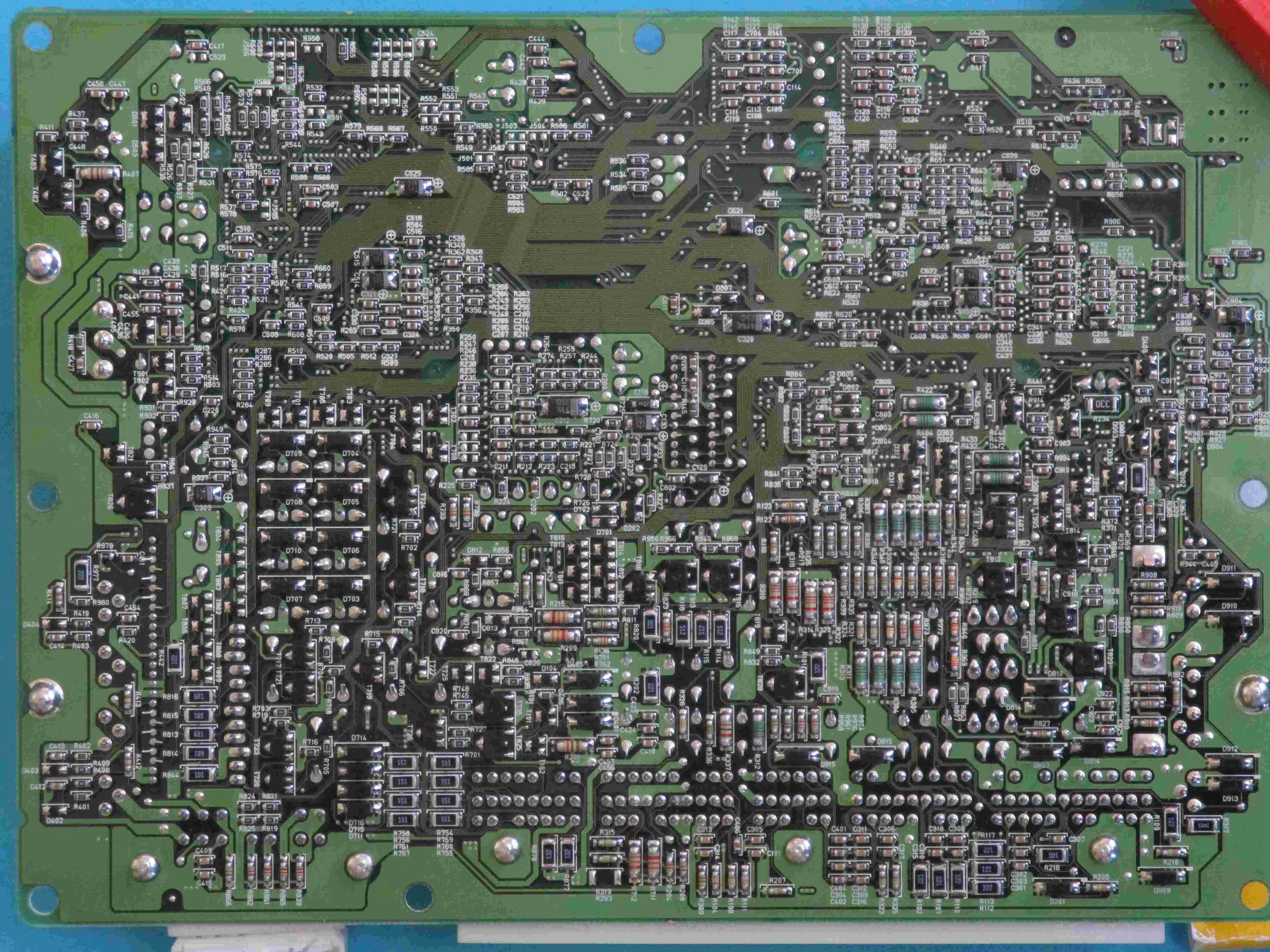
The bottom side of the PCB does not have any ICs, just a mix of discrete components. The PCB appears to be a 3 or 4 layer design, with most of the signal tracks on the top and bottom layers, and power connectivity/ground plane(s) for the internal layer(s).
One of the first tasks to be completed in any analysis is to identify the CPU used. In this case the two large ICs are the most likely suspects, and they both have the same marking of D151851-3830, which is a Denso proprietary designation.
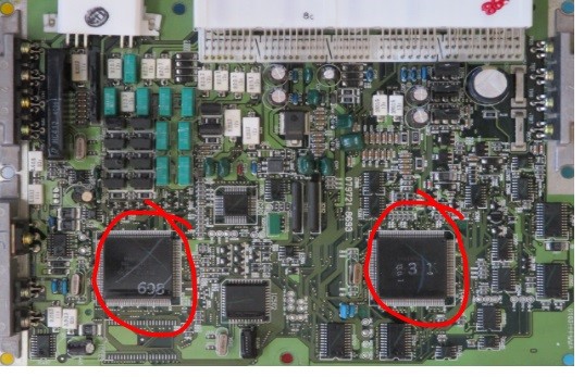
An academic paper written at the launch of the AJ26 engined cars provides a clue, stating that two Motorola 68HC16 processors were used, and the AJ27 is known to be an evolution of the AJ26. Another clue is that both the chips have test pads marked for a 10 pin connector, and this matches the configuration used for the Motorola Background Debug Mode (BDM) programming/debugging interface. An internet search of the part number leads to openecu.org, and a discussion of the CPU used in the circa 2002 Subaru WRX, which uses the same chip, and identifies it as a Motorola MC68HC916Y5.
The Y5 variant (and the Y6 which also is also used for some of the production run) has 164 kbyte flash and 7 kbyte of RAM. THe 6 MHz crystal next to each CPU shows that they are clocked at 24 MHz. The 68HC16 CPU core is common across all variants, with a reference manual available at NXP. The Y5 documentation is not easy to locate, but there is a version in Japanese available at openecu.org forums here. The Y5 is similar to the Y3 variant in many ways, and documentation is also available for this part at NXP. The most notable difference between Y3 and Y5 is the RAM-buffered SPI (RSPI) module used on the Y5, which allows sharing of RAM memory between the two CPUs, and is key for the dual processor ECU design. More reference material can also be found here
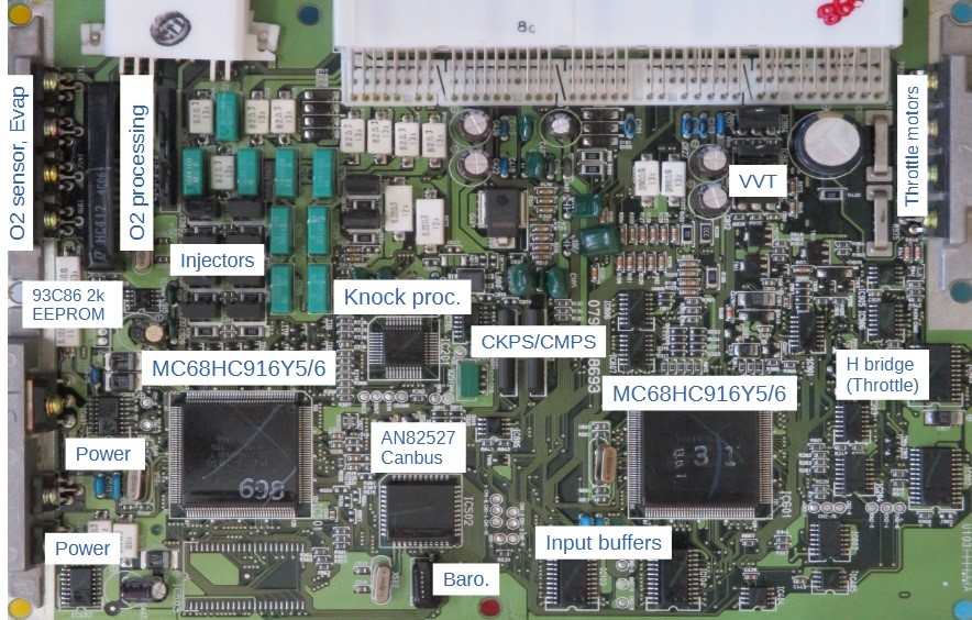
Other important chips used in the ECU are an Intel AN82527 for canbus interface, and a 93C86 2kbyte EEPROM used for persistent data storage. Several other ICs used in the ECU are also Denso proprietary parts, such as for input buffering, power supply control, oxygen sensor processing, knock sensor processing, etc. A rough view of the chips and functions is shown below.
When analyzing the ECU, it is very helpful to know the connectivity between the engine sensors and actuators, and the CPU input/output pins. If the PCB is multi-layer then many of the tracks are hidden in internal layers, and this makes tracing very challenging. For older ECUs such as this one, the vast majority of signal tracks are exposed on the top and bottom layers. High resolution images can help with tracing, and if the components are removed (assuming a spare ECU is available) the task is simplified. Tools for PCB reverse engineering, such as Kicad, can greatly assist in generating a circuit schematic. If a schematic can be created, then when combined with manufacturer electrical guides such as these posted at jagrepair.com, a summary of CPU input/output connectivity can be collated.
In the next post I’ll review a few of the features of the AJ27 design.