Writing a Ghidra processor specification part 2
Following on from part1 of creating a Sleigh spec for 68HC16, the next task is the representation of the CPU instruction set.
Ghidra will fetch bytes of code, and attempt to match them to a specific instruction or group of instructions, using the SLEIGH descriptions. If there is no unique match with the first byte, another byte is read, and so on. Once the instruction has been uniquely identified (Opcode has been matched), then more bytes may be read (Operands) (such as a target address, etc.), as required, in order to execute the instruction. So the key part of a SLEIGH implementation is defining patterns for pattern matching. Finding groups of instructions that use similar patterns allows for efficient coding of SLEIGH instructions. Often, the CPU designers will have grouped similar instructions together and assigned them instruction codes that match a pattern. A study of the instruction codes will typically reveal these patterns. Before looking into more detail around these groupings and patterns, a framework for capturing them needs to be defined.
Sleigh tokens assist in matching patterns. We can focus on, and isolate, certain bits and/or groups of bits within an opcode byte(s) or an operand byte(s) and match these to different patterns. To do this, we define the possible bits/groups of bits we are interested in, for both opcodes and operands/data. For the HC16, opcodes are 1 byte (with or without a prefix), and individual operands are 1 or 2 bytes, and there can be several of them for one instruction. So we define a single byte token for opcodes, and 1 and 2 byte tokens for operands, as follows:
define token opbyte8 (8)
 op8    = (0,7)
 op7_7 = (7,7)
 op6_6 = (6,6)
 op7_6 = (6,7)
 op7_4 = (4,7)
 op7_2 = (2,7)
 op7_1 = (1,7)
 op5_4 = (4,5)
 op5_4a = (4,5)
 op5_4b = (4,5)
 op3_0 = (0,3)
 op1_1 = (1,1)
 op0_0 = (0,0)
;

define token data8 (8)
imm8  = (0,7)
imm8a  = (0,7)
mask8 = (0,7)
simm8 = (0,7) signed
imm0a = (0,0)
imm1a = (1,1)
imm2a = (2,2)
imm3a = (3,3)
imm4a = (4,4)
imm5a = (5,5)
imm6a = (6,6)
imm7a = (7,7)
imm0c = (0,0)
imm1c = (1,1)
imm2c = (2,2)
imm3c = (3,3)
imm4c = (4,4)
imm5c = (5,5)
imm6c = (6,6)
imm7c = (7,7)
imm0_1 = (0,1)
imm0_2 = (0,2)
imm0_3 = (0,3)
imm0_4 = (0,4)
imm0_5 = (0,5)
imm0_6 = (0,6)
;

define token data16 (16)
imm16  = (0,15)
imm16a = (0,15)
simm16 = (0,15) signed
;
For instance, the opcode token, opbyte8, is defined to allow us to examine various groupings of bits, such as bit 7 only (op7_7), bits 4 and 5 (op4_5), and so on as necessary to facilitate various pattern matching tasks. Once tokens have been defined, parsing instructions to match to patterns can proceed.
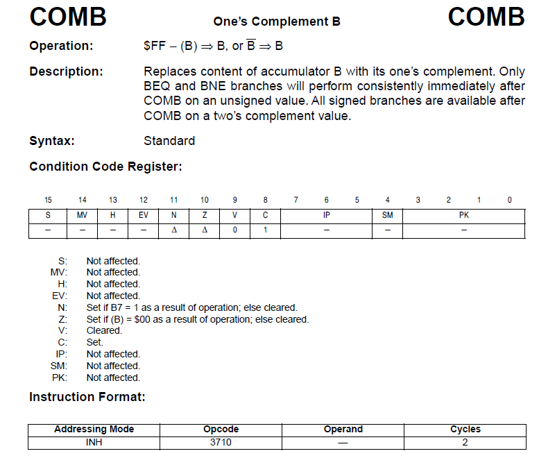
The Sleigh code for HC16 instruction COMB, which has the 2 byte opcode 0x37 0x10, is:
:COMB is prefix=3 & op8=0x10
{
B = ~B;
C = 1;
processFlags1(B);
}
Ghidra will read the first byte, and attempt to match it to patterns defined under each possible instruction. The first byte is handled by a special process, addressed in the next paragraph below (the special process reads the prefix 0x37 and sets the value of the variable “prefix” to 3). Then the next byte is read, and for the instruction COMB (complement register B), a match is obtained if all 8 bits (op8 specifies all 8 bits of the opcode byte) matches the value 0x10. The code inside the {} brackets then specifies what actions are to be taken for this instruction (complement the value of the B register, set the carry flag, update other flags as appropriate using the macro processFlags1).
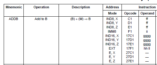
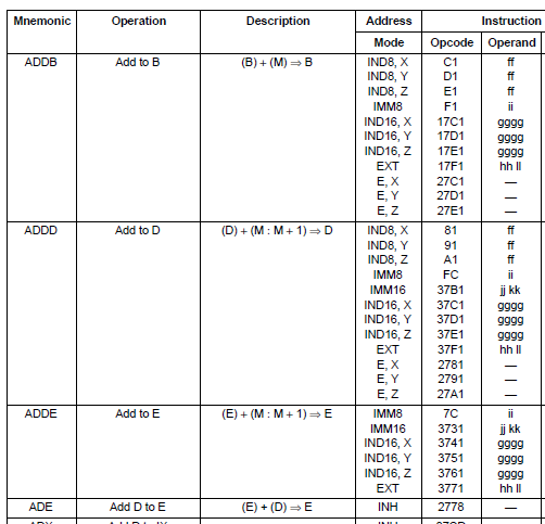
Sometimes, manufacturers have implemented backwards compatibility between different generations of processors in a family, to make code migration simpler. The HC16 16 bit processor is an evolution from the earlier HC11 8 bit processor. A basic HC11 instruction uses a single byte opcode for an instruction, allowing for 256 possible codes. To add more instructions for the HC16 without changing the existing definitions for HC11, 3 additional ‘pages’ were added, using prefixes of 0x17, 0x27 and 0x37 preceding a single byte opcode. For the ADDB instruction above, the IND8 and IMM8 addressing modes use a single byte opcode. The IND16 and EXT addressing modes use the 0x17 prefix before the single byte opcode, and the E mode uses the prefix 0x27. SLEIGH allows us to examine a byte, and match it one of the four pages (none, 0x17, 0x27, 0x37). Once this pattern is matched, we can strip off the prefix if there is one, and continue to match the pattern with the next opcode. This recursive approach to pattern matching is achieved using the special “instruction” keyword, see here for more details. To use this technique, we define a ‘dummy’ register (called ‘contextreg’) that can maintain state information about the processor.
define register offset=0xC0 size=4 contextreg;
define context contextreg
  phase=(0,0)    # 0:initial, 1:instruction-parse
  prefix=(1,2)   # 0:none, 1: 0x17, 2:0x27, 3:0x37)
- bit 0 of contextreg is defined as a field called ‘phase’, and can have 2 values, 0 or 1)
- bits 1-2 of contextreg are defined as a field called ‘prefix’, and can have one of 4 values: 0,1,2 or 3) (see here as to why size=4)
When parsing an opcode, before doing anything else (phase = 0), we test if the opcode matches 0x17,27,37,or other. We then update the prefix value to be 1,2,3,or 0 accordingly. And we update the phase value to be 1. We then apply instruction matching patterns to the next opcode (phase = 1). This is coded as below:
:^instruction is phase=0 & op8=0x17 ;  instruction [ prefix=1;  phase=1;]  { }
:^instruction is phase=0 & op8=0x27 ;  instruction [ prefix=2;  phase=1;]  { }
:^instruction is phase=0 & op8=0x37 ;  instruction [ prefix=3;  phase=1;]  { }
:^instruction is phase=0 & instruction [ prefix=0; phase=1;]  { }
In this way, we are able to read the instruction page prefix first, and then proceed to examine the next opcode in combination with knowledge of the current prefix value. This helps us deal with instructions that are either one or two byte opcodes, and reduce all matching to a single opcode plus a prefix value, which simplifies Sleigh coding. So for the COMB instruction example earlier in this post, we can apply the matching criteria “prefix=3 & op8=0x10”
The other major concept we need to address is how to deal with all the different addressing modes for a single instruction. A good objective (although not always possible or efficient) is to attempt to code an instruction only once for all possible patterns. This means that the code only has to be maintained in one place for bug fixes, etc. Note that this is a design choice only, and it is perfectly acceptable to write a sleigh description for each different address mode of each instruction. As we have seen, instructions often have multiple opcodes, to accommodate multiple addressing modes for specifying target addresses. The opcode mappings created by the manufacturer often incorporate patterns that consistently specify the different modes.
For the HC16, addressing modes include:
- Immediate 8 bit
- Immediate 16 bit
- Indexed 8 bit using X,Y,or Z index register and 8 bit unsigned offset
- Indexed 16 bit using X,Y,or Z index register and 16 bit signed offset
- Extended with 16 bit address and 4 bit extension
- Accumulator offset using X,Y,or Z index register and 16 bit signed offset from E register
Study of the opcodes reveal that opcode bits 4,5 usually indicate the index register to use across a wide group of instructions, etc.
- 00 for X
- 01 for Y
- 10 for Z
- 11 for extended address
SLEIGH allows us to define a “table” to match these patterns. Consider the ASL instruction:
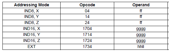
Ignoring the prefix, the opcode bit patterns are:
- 0x04 : 00 00 0100
- 0x14 : 00 01 0100
- 0x24 : 00 10 0100
- 0x34 : 00 11 0100
So we can specify:
- Prefix=0 for for IND8 mode, and Prefix=1 for IND16/EXT mode
- Matching the opcode to 00 xx 0100 gives the ASL instruction (i.e. match bits 7,6,3,2,1,0
- Matching the opcode to xx 00 xxxx indicates X register, 01 for Y register, etc. (i.e. match bits 5,4)
A further study of the instruction set will reveal that this pattern can be applied to 11 instructions (ASL, ASR, CLR, COM, DEC, INC, LSR, NEG, ROL, ROR, TST) which all manipulate one byte in memory. We can define a new table, which we call “memByte1”, which matches to the target patterns for the 11 instructions in this grouping. Table “memByte1” will allow us to identify which of the 7 addressing modes is used, and allow us to calculate the target address of the memory byte from the instruction operands. It will also help create the information required to display the instruction in the disassembly listing window in Ghidra. Three entries will be needed for the table, for the three supported address modes, namely IND8, IND16, and EXT modes.
Using the token opbyte8 that we defined earlier, shown below,
define token opbyte8 (8)
 op8    = (0,7)
 op7_7 = (7,7)
 op6_6 = (6,6)
 op7_6 = (6,7)
 op7_4 = (4,7)
 op7_2 = (2,7)
 op7_1 = (1,7)
 op5_4 = (4,5)
 op5_4a = (4,5)
 op5_4b = (4,5)
 op3_0 = (0,3)
 op1_1 = (1,1)
 op0_0 = (0,0)
;
we can use op5_4 to extract the value of bits 5 and 4, which we have seen specify the index register to be used to compute the target address (X, Y, or Z). We define 3 tokens for bits 5 and 4 (op5_4, op5_4a, op5_4b) since we have 3 different tasks to perform using these two bits.
- Task 1 is extracting the actual value stored in the register
attach variables [op5_4a] [IXE IYE IZE _ ];
- Task 2 is creating text representing the register for the disassembly display.
attach names [op5_4b] ["X" "Y" "Z" "Unknown"];
- Task 3 is defining the opcode patterns we are interested in, creating the display text for the register, and computing the target address. We do this by defining a Sleigh ‘table’ called “indexReg”. This is a primitive, or ‘helper’ table, that we use to help us build up the final ‘memByte1’ table.
indexReg: op5_4b is (op5_4=0b00 | op5_4=0b01 | op5_4=0b10) & op5_4a & op5_4b
{ local addr:4 = op5_4a:4 ; export addr;}
We can define similar, but simpler, primitive tables to help us with the IND8, IND16 and EXT address modes, as follows, refering to the ASL instruction as a reference.
- IND8 operand is 1 byte, an 8 bit unsigned value, which will get added to the X, Y or Z register
offset_u8: imm8 is imm8
{ local addr:4 = zext(imm8:1); export addr;}
- IND16 operands is 2 bytes, a 16 bit signed value, which will get added to the X, Y or Z register
offset_s16: simm16 is simm16
{ local addr:4 = sext(simm16:2); export addr;}
- EXT operand is 2 bytes, a 16 bit unsigned value, which combined with the extension register (4 bit extension to 20 bits)
extendedAddr: imm16	is imm16
{ local addr:4 = zext(imm16:2) + EK; export addr;}
We can then use these primitives, or helper tables, to create the ‘Membyte1’ table, which has 3 entries corresponding to the 3 addressing modes (IND8, IND16, EXT) as follows:
memByte1: offset_u8,indexReg is prefix=0 & indexReg ; offset_u8 { local addr:4 = indexReg + offset_u8; export *:1 addr; }
memByte1: offset_s16,indexReg is prefix=1 & indexReg ; offset_s16 { local addr:4 = indexReg + offset_s16; export *:1 addr; }
memByte1: extendedAddr is prefix=1 & op5_4=0b11 ; extendedAddr { local addr:4 = extendedAddr; export *:1 addr; }
A easier to read screenshot of memByte1 rendered using Eclipse Sleigh editor with code highlighting is:

The first entry, for IND8, uses indexReg table to determine the target register from the opcode, and offset_u8 table to get the offset. These are then added to compute the target 32 bit memory address. We can then set the value of memByte1 to the byte value stored at this address in memory. The coding export *:1 addr does this - ‘export’ assigns the value of variable memByte1 to the 1 byte value (:1) contained in the memory location (*) at the 32 bit/4 byte address “addr:4”. The second and third entries for IND16 and EXT use similar coding.
Having defined the table ‘memByte1’, we can now create a single entry for the Sleigh description of the ASL instruction which covers all its addressing modes.
:ASL memByte1	is (op7_6=0b00 & op3_0=0b0100 & (prefix=1 | $(NotPrefix0AndOp54))) ... & memByte1
{
tmp:1 = memByte1;
C = (tmp s< 0);
tmp = tmp << 1;
memByte1 = tmp;
shiftFlags(tmp);
}
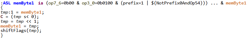
Matching both op7_6 and op3_0 determines the target instruction from the group of 11 using this pattern. The additional constraints prefix=1 and macro NotPrefix0andOp54 ensure no overlap versus parsing other HC16 instructions. This is because the addressing tables for different modes may overlap, depending on the specific patterns needed.
The ellipsis (…) symbol is required because the patterns/address modes specified in memByte1 table are of various lengths. IND8 is 2 bytes (after prefix stripping), IND16 and EXT are 4 bytes. memByte1 is used for parsing both the opcode and the operands, so it can be applied to either 2 or 4 bytes of code. The constraints (op7_6=0b00 & op3_0=0b0100 & (prefix=1 | $(NotPrefix0AndOp54))) are on the single opcode byte only - they all only apply to a single byte token. So this section is extended/padded with ‘dummy’ additional bytes to the right as necessary, using the ellipsis symbol, in order to match the size of the second part of the matching criteria, namely the memByte1 table.
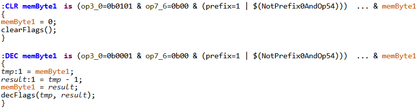
The memByte 1 table can then also be used for other instructions from the same group of 11, such as CLR, DEC, etc.
In the next post, we’ll review the other addressing modes, branching, the other required files for the processor module (.ldefs, .pspec, etc.), and compiling and installing the processor module into Ghidra.