Writing a Ghidra processor specification part 1
To analyze 68HC16 code using Ghidra, we need to write a processor specification in Ghidra’s SLEIGH language. The first step is to assemble to software tools needed for the development environment. If starting from scratch, you will probably need to install:
- Java Development Kit (e.g. Adoptium)
- Eclipse IDE (for Java Developers)
- Ghidra
- GhidraDev extension for Eclipse IDE
The Ghidra installation guide should provide up to date instructions on getting Ghidra up and running. Once Ghidra has been installed, the “docs” folder in the Ghidra installation has good information on learning and using Ghidra (in: docs > GhidraClass), as well as details on the SLEIGH processor specification language (in: docs > languages). Likewise, there are instructions in the “Extensions > Eclipse” folder on installing GhidraDev. One additional resource that is very informative is The Ghidra Book which provides many insights into using and extending the Ghidra tool.
Once the development environment is up and running, the first task is to familiarize yourself with the architecture of the target processor, in this case the 68HC16.
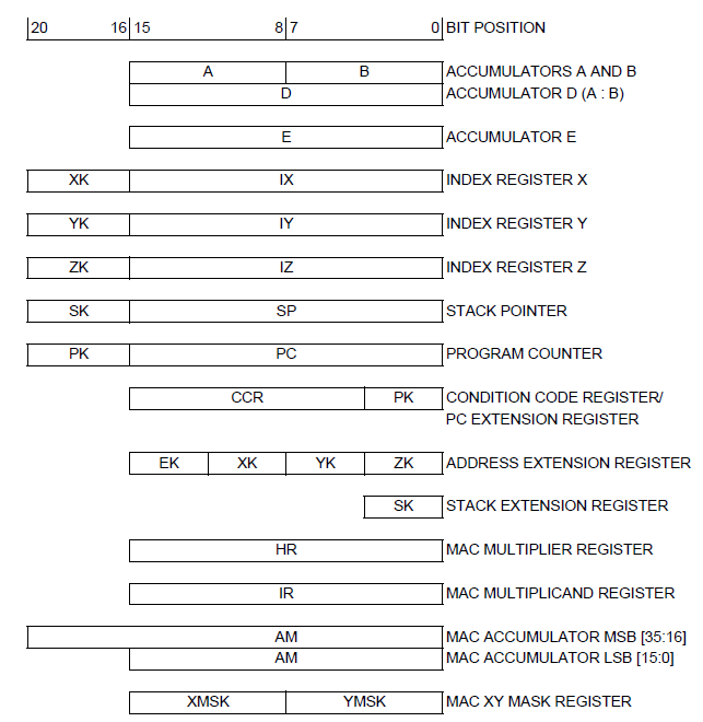
As can be seen above, there are a number of general and specialized registers, and these will need to be modeled in SLEIGH.
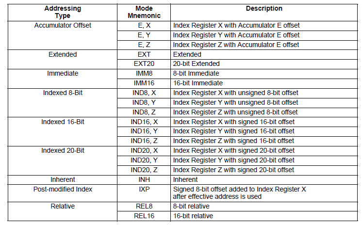
Additionally there are a number of different addressing modes to access data memory, and these will also need to be modeled.
In order to create a new project for a processor model, the steps (as of time of writing) are:
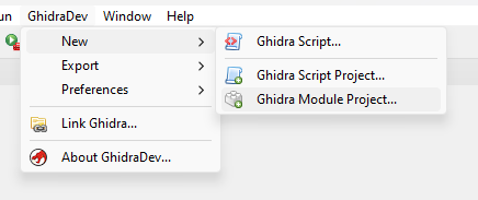
In Eclipse, click “GhidraDev > New > Ghidra Module Project” menu item
Enter a suitable name in the “Project Name:” field, e.g. MC68HC16, and click “Next >”
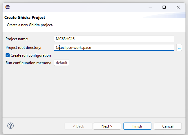
Unselect all module templates except “Processor”, and click “Finish”
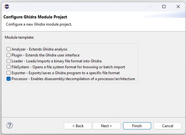
A new project will be created and visible in the Package Explorer Window. Expand the folder data > languages, and there will be a set of ‘skeleton’ example files (skel.*)
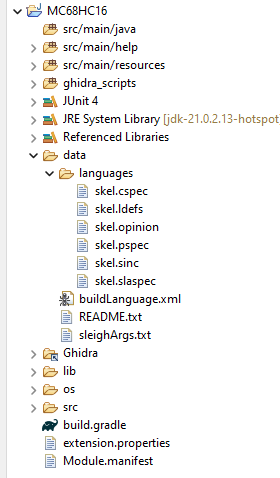
These provide some examples/guidance of typical content that will be required in each file – but they are not typically used ‘as is’. So either rename, or delete and create new files with useful names:
- Right click on file, Refactor > Rename… skel.cspec to MC68HC16.cspec, and so on for .pspec, .ldefs, .sinc, .slaspec The .opinion file can be deleted
or
- Right click on file and delete, then right click on “languages’ folder and select > New, then > File from drop down list, and give the file a relevant name, like MC68HC16.cspec Repeat for .pspec, .ldefs, .sinc, .slaspec
The roles of these different files are:
- .cspec – compiler specification, used as guidance for decompiling code to a C representation (most useful if the code was actually written in a high level language/C variant, as opposed to native assembler)
- .ldefs – language definition (contains references for the required files - .sla .pspec, etc., and also some basic parameters)
- .opinion (not required for simple implementations, related to identification of Ghidra Loaders to use under different conditions)
- .pspec – processor specification (for simple cases needs minimal content)
- .sinc – contains optional SLEIGH specifications to be included in the .slaspec, typically used to describe different variants of a processor
- .slaspec – primary file that contains the SLEIGH specification for the processor
A SLEIGH description of a processor defines how a specific processor instruction set is translated into P-code. And P-code is a generic processor language that models processor instructions. So, similar to the real processor, Ghidra reads bytes of code, and matches them to a specific instruction using the SLEIGH description. This SLEIGH description also defines how to create a P-Code representation of that instruction, and how to display the instruction in a Ghidra disassembly listing window. Since P-Code models instructions, Ghidra can not only analyze code, but it can also emulate running the code, which can be useful to explore routines that are hard to decipher.
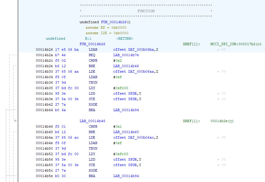
One of the many views that Ghidra can create is a disassembly listing window. If we take a look at the last line we have the following entries:
- 00014b5e - this is the address where the code bytes are stored
- b0 30 - these are the bytes that define the instruction “Branch Always”
- BRA - “Branch Always” is represented with the Mnemonic “BRA”
- LAB_00014b94 - A Label created by Ghidra to represent the address to branch to (address 14b94)
If we consult the 68HC16 processor reference guide, we see that for the BRA instruction we have:
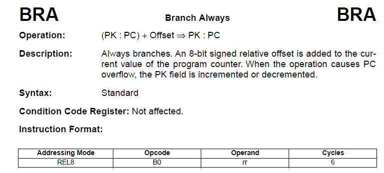
This details that the instruction is represented by the code b0, and the target address to branch to is computed using the operand 30 based on REL8 addressing mode. The Sleigh description will contain entries for each instruction, and inform Ghidra how to take the code bytes b0 30 and interpret them so as to create the disassembly listed as above.
When starting on a Sleigh description (after reading the Ghidra SLEIGH manual several times over), some initial concepts to consider are:
- How data values are represented
- What bit widths should be used for instructions and addressing
- How to represent the processor registers and flags
For the 68HC16 processor, an example approach is:
- big endian data representation - this is defined in the HC16 spec.
- the HC16 is a 16 bit processor, but is an evolution of earlier HC series processors, and so processes code at a byte (8 bit) level, not as words (16 bit) or bigger chunks
- addresses are 20 bits in practice (64 pages of 16 bits, or 4+16 bits) (even if the processor has 24 address lines/bits). To keep things simple, we can allocate 32 bits (4 bytes) of address space, although using 24 bits will also work
- The HC16 can use separate, or combined, data and program address spaces. The implementation will focus on combined, and worry about separation later if needed. To keep things simple, we will allocate 16 bits (2 bytes) of register space
This leads to the following initial lines in the processor module.
define endian=big;
define alignment=1;
define space code type=ram_space size=4 default;
define space register type=register_space size=2;
Next we need to consider how to represent the various registers. SLEIGH uses byte based values, so trying to represent anything using less than one byte is not really helpful (even if accurate bit by bit representations are also created where necessary). The HC16 creates effective addresses by combining base and extension registers (e.g. the 16 bits from IX plus the 4 XK bits from the address extension register), so it is useful to model these 20 bit ‘virtual’ registers even though they don’t exist in the actual processor. Note also that SLEIGH is efficient in modeling ‘overlapping’ registers, such as the example D (2 bytes) is a combination of A and B (1 byte each). Considering all these points, a representation of the registers is:
define register offset=0x00 size=1 [A B];
define register offset=0x00 size=2 [D];
define register offset=0x02 size=2 [E];

define register offset=0x10 size=4 [IXE IYE IZE];
define register offset=0x10 size=2 [_ IX _ IY _ IZ];
define register offset=0x10 size=2 [XKE _ YKE _ ZKE];

define register offset=0x20 size=4 [SPextended];
define register offset=0x22 size=2 [SP];
define register offset=0x20 size=2 [SP_EXT];

define register offset=0x30 size=4 [PCextended];
define register offset=0x32 size=2 [PC];

define register offset=0x40 size=2 [CCR_PK];
define register offset=0x42 size=1 [SM IPF C V Z N EV H MV S SignLatch];

define register offset=0x50 size=2 [K];
define register offset=0x52 size=4 [EK];

define register offset=0x60 size=2 [HR IR];

define register offset=0x70 size=5 [AMFull];
define register offset=0x70 size=1 [AM_MSB];
define register offset=0x71 size=2 [AM_MidW];
define register offset=0x73 size=2 [AM_LSW];
define register offset=0x70 size=3 [AM_Top3];

define register offset=0x80 size=2 [XYMSK];
define register offset=0x80 size=1 [XMSK YMSK];
One way of ensuring bit-accurate representations of registers are maintained (such as required during emulation) is to synchronize them with their byte by byte representations whenever any values change, such as by the use of macros. For example, condition code flag bits can be sync’d with their byte representations, and 4 bit extension register values can be sync’d with their virtual register representations.
macro syncCCRtoFlags()
{
CCR_PK[15,1] = S;
CCR_PK[14,1] = MV;
CCR_PK[13,1] = H;
CCR_PK[12,1] = EV;
CCR_PK[11,1] = N;
CCR_PK[10,1] = Z;
CCR_PK[9,1] = V;
CCR_PK[8,1] = C;
CCR_PK[5,3] = IPF[0,3];
CCR_PK[4,1] = SM;
CCR_PK[0,4] = PCextended[16,4];
}

macro syncFlagsToCCR()
{
S = CCR_PK[15,1];
MV = CCR_PK[14,1];
H = CCR_PK[13,1];
EV = CCR_PK[12,1];
N = CCR_PK[11,1];
Z = CCR_PK[10,1];
V = CCR_PK[9,1];
C = CCR_PK[8,1];
IPF = CCR_PK[5,3];
SM = CCR_PK[4,1];
}

macro buildK()
{
K[12,4] = EK[16,4];
K[8,4] = XKE[0,4];
K[4,4] = YKE[0,4];
K[0,4] = ZKE[0,4];
}

macro syncToK()
{
EK = zext(K[12,4]) << 16;
XKE = zext(K[12,4]);
YKE = zext(K[4,4]);
ZKE = zext(K[0,4]);
}
Now that the basic representation of the CPU architecture has been created, in the next post we’ll move on to the representation of the CPU instruction set.